Your idea, in copper.
Volt Zero is a circuit board editor that runs in your browser. You write the board in a small language with real units; Volt checks and routes it and draws it in 3D. Your agent can edit the same board while you work on it. There’s no account and nothing to install.
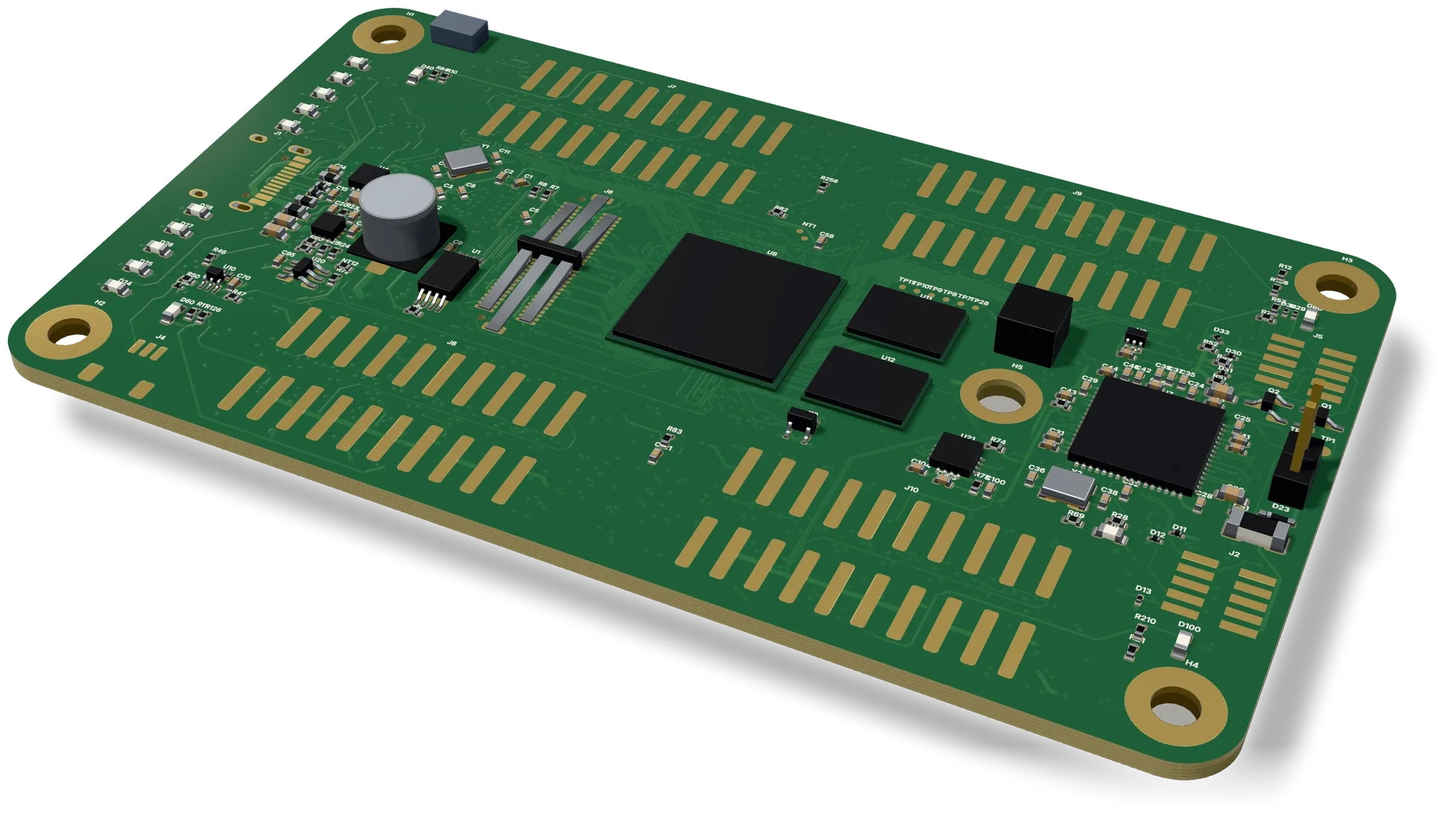
From a sentence to a board, in 36 seconds.
One Rust core, on your machine and in your browser.
Everything Volt does lives in one Rust codebase, from the language to the renderer. It builds into the volt command line, and into WebAssembly for the app.
- Give the router the same work budget and a route comes out byte for byte the same in the browser and on the command line, on any machine and with any number of threads. A test checks this on every fixture board.
- The same renderer draws the board everywhere: on WebGPU or WebGL2 in the browser, and to PNG files from the command line.
- An edit reaches the screen in 4–26 ms on boards up to 6 MB.
A board is a text file you can review in a pull request.
A board is design.volt plus a few block files in a git repository. You say what’s on the board and how it’s connected, and Volt works out where the copper goes. The file below is a real one. It evaluates without errors and routes to completion.
use "blocks/support.volt" as support
net GND, VBUS
net V3 named "+3V3"
net USB_DP, USB_DN
net STATUS
bus I2C[2]
pair USB = (USB_DP, USB_DN)
board = Board {
name = "sensor-node"
outline = rect(50mm, 30mm)
cutouts = [circle((3.5mm, 26.5mm), 1.6mm), circle((46.5mm, 26.5mm), 1.6mm)]
layers = [signal(Cu.top), signal(Cu.bottom)]
}
usb = NetClass {
trackWidth = 0.2mm
diffPairGap = 0.2mm
nets = [USB]
}
ldo = support.Ldo(VBUS, V3, GND, bulk = 4.7uF) { at = (14mm, 24mm) }
U1 = Mcu {
at = (25mm, 14mm)
pins { VDD: V3, DP: USB.p, DN: USB.n, SDA: I2C[0], SCL: I2C[1], LED: STATUS, GND: GND }
}
status = support.StatusLed(STATUS, GND) { at = (34mm, 6mm) }
sensor = support.SensorPort(V3, I2C[0], I2C[1], GND) { at = (46mm, 15mm) }
gnd = pour(net = GND, layers = [Cu.bottom]) { outline = board.outline }
rule UsbPair {
select = copper(pair = USB)
limits { trackWidth: limit(min = 0.2mm), diffPairGap: limit(min = 0.15mm, max = 0.25mm) }
}
Show the whole file (78 lines)
use "blocks/support.volt" as support

// USB-powered sensor node: 3.3 V regulator, QFN-32 MCU, I2C sensor port and SWD port.
net GND, VBUS
net V3 named "+3V3"
net USB_DP, USB_DN
net STATUS
bus I2C[2]
pair USB = (USB_DP, USB_DN)

board = Board {
  name = "sensor-node"
  outline = rect(50mm, 30mm)
  cutouts = [circle((3.5mm, 26.5mm), 1.6mm), circle((46.5mm, 26.5mm), 1.6mm)]
  layers = [signal(Cu.top), signal(Cu.bottom)]
}

supply = NetClass {
  trackWidth = 0.5mm
  nets = [VBUS, V3, GND]
}
usb = NetClass {
  trackWidth = 0.2mm
  diffPairGap = 0.2mm
  nets = [USB]
}

part Mcu = device(footprint = qfn(32, size = (5mm, 5mm), ep = (3.1mm, 3.1mm)), pinout = {
  VDD: ["1", "17"],
  DN: "3",
  DP: "4",
  NRST: "8",
  SDA: "21",
  SCL: "22",
  LED: "24",
  SWDIO: "29",
  SWCLK: "30",
  GND: "33",
})
part C100n = cap(100nF, package = "0402") // one per supply pin

J1 = header(4) {
  at = (4mm, 15mm)
  pins = [VBUS, USB.n, USB.p, GND]
}
ldo = support.Ldo(VBUS, V3, GND, bulk = 4.7uF) { at = (14mm, 24mm) }

U1 = Mcu {
  at = (25mm, 14mm)
  pins { VDD: V3, DP: USB.p, DN: USB.n, SDA: I2C[0], SCL: I2C[1], LED: STATUS, GND: GND }
}

decoupling = {
  for ((i, p) in enumerate([(21mm, 17mm), (29mm, 11mm)])) {
    [i]: C100n { at = p; rotation = 90deg; pins { a: V3, b: GND } },
  }
}

J3 = header(5, pitch = 1.27mm) {
  // debug port, joined to the MCU's pins directly
  at = (25mm, 3mm)
  rotation = 90deg
  pins = [V3, U1.pin.SWDIO, U1.pin.SWCLK, U1.pin.NRST, GND]
}
R1 = res(10kohm, package = "0402") {
  at = (20mm, 8mm)
  pins { a: V3, b: U1.pin.NRST }
}

status = support.StatusLed(STATUS, GND) { at = (34mm, 6mm) }
sensor = support.SensorPort(V3, I2C[0], I2C[1], GND) { at = (46mm, 15mm) }

gnd = pour(net = GND, layers = [Cu.bottom]) { outline = board.outline }

rule UsbPair {
  select = copper(pair = USB)
  limits { trackWidth: limit(min = 0.2mm), diffPairGap: limit(min = 0.15mm, max = 0.25mm) }
}
Units
Every value has a dimension: 0.5mm, 100nF, 10kohm, 90deg. Add millimetres to nanofarads and you get an error on that line.
Typed nets and pins
Nets, buses and differential pairs, with pins checked by name. Connect two nets by mistake and Volt reports a short.
Parts and blocks
A part is something you buy. A block is a reusable circuit with parameters and its own coordinate frame.
Footprints, computed
82 land patterns, computed from package dimensions per IPC-7351B. Of 14 checked against a reference library, 13 match pad for pad to within 1 µm.
Classes, rules, pours
Net classes, typed rules with selectors, keepouts and rule areas. Copper pours get thermal reliefs.
Room to move
Say where a part may move, how it may rotate and which pins may swap, and the tools stay within those limits.
There’s a formatter and a language server too, so you get errors, hover, completion and go-to-definition in your editor as well as in the app.
Route the same board twice and you get the same copper.
The router is a deterministic search. Most of its work comes from the six ideas below, and all of them are on by default.
Negotiate
All nets are routed at once, overlapping at first. Each pass makes contested space more expensive, until no two nets share it. The search grid has eight directions and spans every layer.
Exact where it counts
The grid guides the search, but every clearance is checked against exact geometry, to a fraction of a micron. Fine-pitch escapes with zero slack still fit.
Search the neighbourhood
Next it rips up a window around whatever is still unrouted, routes it again and keeps the result if it is better. Eight candidate states are searched side by side.
Pours, live
Copper pours are modelled while routing: the fill, the clearance around other nets, islands and thermal spokes. The router knows which pads a pour actually connects.
Pad access as a set
A pad on a dense part gets up to eight exact, full-width exits. Neighbouring pads negotiate for them instead of each getting a fixed stub.
Respects the mask
It knows where the solder mask opens, which vias are untented and where thin mask webs sit between pads, and routes so the fab can keep them.
Measured against an independent checker.
We measure every change to the router, the checks and file import on public boards that people designed. A separate design-rule checker judges the result, and a board only counts if it comes out clean.
96.1%
of 482 curated public boards import and export with every pad and every connection confirmed by an independent checker
standard open board files, both ways
232/235
human-designed boards where, after a refill, pour connectivity matches the independent checker
copper pours
4–26ms
from an edit to the board on screen, on boards up to 6 MB, in the browser
measured in a headless browser
13/14
reference footprints matched pad for pad to 1 µm by footprints computed per IPC-7351B
footprint library
Your agent works in the same app.
Use the agent you already have: Claude Code, Codex, OpenCode, Cursor, Gemini CLI, or anything else that can drive Chrome over the DevTools Protocol, an extension or a script. It doesn’t click around the interface or read pixels. It calls an API on the page with the same commands you run from the palette.
- Each command has a JSON Schema for its input and output, and says what it changes.
- A journal shows what changed since the agent’s last turn. Long tasks run as jobs. The agent can also see your view, down to what you’ve selected, and every change it makes can be undone.
- The app’s
/agents.mdand/llms.txtare generated from the commands. Browsers with WebMCP get the commands as tools.
volt.hello("my-agent")
await volt.commands("route")          // what it does, its schema
await volt.call("route", {})          // runs as a job
await volt.wait("job")
await volt.call("view.state", {})     // what the person sees
await volt.call("journal.since", {})  // what changed since my turn
From a terminal, the volt command line runs the same commands.
No account and nothing to install.
Open it and start
Go to app.volt0.ai. There’s no sign-up, and once the page has loaded it keeps working offline.
Your files stay with you
Open a board’s git repository from a folder on your computer and edit it in place, or keep the project in the browser’s storage.
Nothing on our servers
Checks, routing, import and export run on your machine in WebAssembly workers. Your project only leaves it when you export it.
From a sentence to a board you can hold.
Tell your agent what the board should do. It writes the design, Volt routes it, and you watch it take shape in 3D. Today a finished board leaves Volt in the standard open board file format, with its project and rules, so you can use the fab tools you already have.
We’re working on the rest: Gerber and drill files, a bill of materials and pick-and-place for assembly, and ordering from JLCPCB inside the app.
Say what you need
“A USB sensor node, 50 × 30 mm, two layers, an I2C port.”
Your agent writes the design
Parts and where they sit, nets and rules, in design.volt. Volt checks it as it is written.
Volt routes it
Every net, the same way every time, until the checks come out clean. You see the board in 3D.
Fabrication filesnext
Gerber for every layer and the outline, drill files, a bill of materials and pick-and-place.
Order the boardnext
Finish, mask colour, copper weight and quantity, checked against what the fab can make, and sent to JLCPCB from the app.
Your idea, in copper.
In your browser. No sign-up, nothing to install.
Who makes it
I’m Sergey Alekseev. I’m also building Rabbit, an autonomous rover, and I write about it atrabbit0.dev. Volt started as the tool I wanted for Rabbit’s boards, something my agent and I could both work in.